
Scientists have predicted that by 2040, nearly 50 p.c of the world’s electrical energy will likely be utilized in computing. What’s extra, this projection was made earlier than the sudden explosion of generative AI. The quantity of computing sources used to coach the biggest AI fashions has been doubling roughly every 6 months for greater than the previous decade. At this fee, by 2030 coaching a single artificial-intelligence mannequin would take 100 instances as a lot computing sources because the mixed annual sources of the present top ten supercomputers. Merely put, computing would require colossal quantities of energy, quickly exceeding what our planet can present.
One technique to handle the unsustainable power necessities of the computing sector is to essentially change the way in which we compute. Superconductors might allow us to do exactly that.
Superconductors provide the potential of drastically decreasing power consumption as a result of they don’t dissipate power when passing a present. True, superconductors work solely at cryogenic temperatures, requiring some cooling overhead. However in trade, they provide nearly zero-resistance interconnects, digital logic constructed on ultrashort pulses that require minimal power, and the capability for unimaginable computing density as a result of simple 3D chip stacking.
Are the benefits sufficient to beat the price of cryogenic cooling? Our work suggests they most definitely are. As the dimensions of computing sources will get bigger, the marginal value of the cooling overhead will get smaller. Our analysis reveals that beginning at round 1016 floating-point operations per second (tens of petaflops) the superconducting laptop handily turns into extra energy environment friendly than its classical cousin. That is precisely the dimensions of typical high-performance computer systems right this moment, so the time for a superconducting supercomputer is now.
At Imec, we’ve got spent the previous two years growing superconducting processing items that may be manufactured utilizing normal CMOS instruments. A processor based mostly on this work could be 100 instances as power environment friendly because the most efficient chips today, and it could result in a pc that matches a data-center’s price of computing sources right into a system the scale of a shoebox.
The Physics of Vitality-Environment friendly Computation
Superconductivity—that superpower that permits sure supplies to transmit electrical energy with out resistance at low sufficient temperatures—was found again in 1911, and the concept of utilizing it for computing has been round since the mid-1950s. However regardless of the promise of decrease energy utilization and better compute density, the expertise couldn’t compete with the astounding advance of CMOS scaling beneath Moore’s Regulation. Analysis has continued by means of the a long time, with a superconductingCPU demonstrated by a bunch at Yokohama Nationwide College as not too long ago as 2020. Nonetheless, as an support to computing, superconductivity has stayed largely confined to the laboratory.
To deliver this expertise out of the lab and towards a scalable design that stands an opportunity of being aggressive in the actual world, we needed to change our strategy right here at Imec. As an alternative of inventing a system from the underside up—that’s, beginning with what works in a physics lab and hoping it’s helpful—we designed it from the highest down—beginning with the required performance, and dealing straight with CMOS engineers and a full-stack growth workforce to make sure manufacturability. The workforce labored not solely on a fabrication course of, but in addition software program architectures, logic gates, and standard-cell libraries of logic and reminiscence components to construct an entire expertise.
The foundational concepts behind energy-efficient computation, nonetheless, have been developed as far back as 1991. In standard processors, a lot of the facility consumed and warmth dissipated comes from shifting info amongst logic items, or between logic and reminiscence components somewhat than from precise operations. Interconnects product of superconducting materials, nonetheless, don’t dissipate any power. The wires have zero electrical resistance, and due to this fact, little power is required to maneuver bits throughout the processor. This property of getting extraordinarily low power losses holds true even at very excessive communication frequencies, the place it could skyrocket unusual interconnects.
Additional power financial savings come from the way in which logic is completed contained in the superconducting laptop. As an alternative of the transistor, the fundamental ingredient in superconducting logic is the Josephson-junction loop.
A Josephson junction is a sandwich—a skinny slice of insulating materials squeezed between two superconductors. Join the 2 superconductors, and you’ve got your self a Josephson-junction loop.
Beneath regular situations, the insulating “meat” within the loop is so skinny that it doesn’t deter a supercurrent—the entire sandwich simply acts as a superconductor. Nonetheless, in case you ramp up the present previous a threshold often known as a crucial present, the superconducting “bread slices” across the insulator get briefly knocked out of their superconducting state. On this transition interval, the junction emits a tiny voltage pulse, lasting only a picosecond and dissipating simply 2 x 10-20 joules, a hundred-billionth of what it takes to put in writing a single bit of knowledge into conventional flash memory.
A single flux quantum develops in a Josephson-junction loop by way of a three-step course of. First, a present simply above the crucial worth is handed by means of the junction. The junction then emits a single-flux-quantum voltage pulse. The voltage pulse passes by means of the inductor, making a persistent present within the loop. A Josephson junction is indicated by an x on circuit diagrams. Chris Philpot
The secret’s that, as a result of a phenomenon known as magnetic flux quantization within the superconducting loop, this pulse is all the time precisely the identical. It is named a “single flux quantum” (SFQ) of magnetic flux, and it’s fastened to have a price of two.07 millivolt-picoseconds. Put an inductor contained in the Josephson-junction loop, and the voltage pulse drives a present. Because the loop is superconducting, this present will proceed going across the loop indefinitely, with out utilizing any additional power.
Logical operations contained in the superconducting laptop are made by manipulating these tiny, quantized voltage pulses. A Josephson-junction loop with an SFQ’s price of persistent present acts as a logical 1, whereas a current-free loop is a logical 0.
Info storage, the Josephson-junction-based model of SRAM in CPU cache, additionally shops single flux quanta. To retailer one bit, two Josephson-junction loops must be positioned subsequent to one another. An SFQ with a persistent present within the left-hand loop is a reminiscence ingredient storing a logical 0, whereas no present within the left however a present in the proper loop is a logical 1.
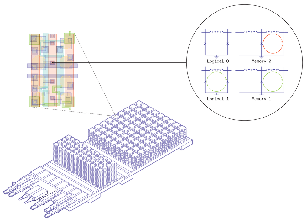 Designing a superconductor-based information heart required full-stack innovation. Imec’s board design incorporates three principal components: the enter and output, main information to the room temperature world, the standard DRAM, stacked excessive and cooled to 77 kelvins, and the superconducting processing items, additionally stacked, and cooled to 4 Ok. Contained in the superconducting processing unit, primary logic and reminiscence components are laid out to carry out computations. A magnification of the chip reveals the fundamental constructing blocks: For logic, a Josephson-junction loop and not using a persistent present signifies a logical 0, whereas a loop with one single flux quantum’s price of present represents a logical 1. For reminiscence, two Josephson junction loops are related collectively. An SFQ’s price of persistent present within the left loop is a reminiscence 0, and a present in the proper loop is a reminiscence 1. Chris Philpot
Progress Via Full-Stack Improvement
To go from a lab curiosity to a chip prototype prepared for fabrication, we needed to innovate the total stack of {hardware}. This got here in three principal layers: engineering the fundamental supplies used, circuit growth, and architectural design. The three layers needed to go collectively—a brand new set of supplies requires new circuit designs, and new circuit designs require novel architectures to include them. Codevelopment throughout all three phases, with a strict adherence to CMOS manufacturing capabilities, was the important thing to success.
On the supplies stage, we needed to step away from the earlier lab-favorite superconducting materials: niobium. Whereas niobium is straightforward to mannequin and behaves very effectively beneath predictable lab situations, it is extremely tough to scale down. Niobium is delicate to each course of temperature and its surrounding supplies, so it’s not appropriate with normal CMOS processing. Subsequently, we switched to the associated compound niobium titanium nitride for our primary superconducting materials. Niobium titanium nitride can face up to temperatures utilized in CMOS fabrication with out dropping its superconducting capabilities, and it reacts a lot much less with its surrounding layers, making it a way more sensible selection.
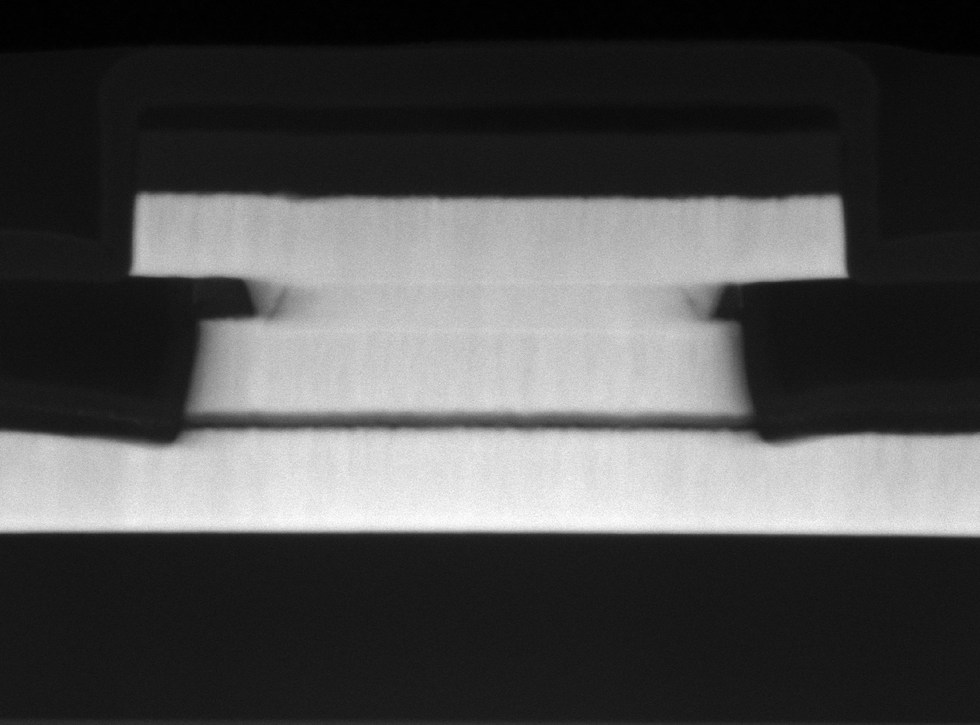 The essential constructing block of superconducting logic and reminiscence is the Josephson junction. At Imec, these junctions have been manufactured utilizing a brand new set of supplies, permitting the workforce to scale down the expertise with out dropping performance. Right here, a tunneling electron microscope picture reveals a Josephson junction made with alpha-silicon insulator sandwiched between niobium titanium nitrite superconductors, reaching a crucial dimension of 210 nanometers. Imec
Moreover, we employed a brand new materials for the meat layer of the Josephson-junction sandwich—amorphous, or alpha, silicon. Typical Josephson-junction supplies, most notably aluminum oxide, didn’t scale down effectively. Aluminum was used as a result of it “wets” the niobium, smoothing the floor, and the oxide was grown in a well-controlled method. Nonetheless, to get to the ultrahigh densities that we’re focusing on, we must make the oxide too skinny to be virtually manufacturable. Alpha silicon, in distinction, allowed us to make use of a a lot thicker barrier for a similar crucial present.
We additionally needed to devise a brand new technique to energy the Josephson junctions that might scale all the way down to the scale of a chip. Beforehand, lab-based superconducting computer systems used transformers to ship present to their circuit components. Nonetheless, having a cumbersome transformer close to every circuit ingredient is unworkable. As an alternative, we designed a technique to ship energy to all the weather on the chip without delay by making a resonant circuit, with specialised capacitors interspersed all through the chip.
On the circuit stage, we needed to redesign the whole logic and reminiscence construction to reap the benefits of the brand new supplies’ capabilities. We designed anovel logic architecture that we name pulse-conserving logic. The important thing requirement for pulse-conserving logic is that the weather have as many inputs as outputs and that the entire variety of single flux quanta is conserved. The logic is carried out by routing the only flux quanta by means of a mixture of Josephson-junction loops and inductors to the suitable outputs, leading to logical ORs and ANDs. To enhance the logic structure, we additionally redesigned a appropriate Josephson-junction-based SRAM.
Lastly, we needed to make architectural improvements to take full benefit of the novel supplies and circuit designs. Amongst these was cooling standard silicon DRAM all the way down to 77 kelvins and designing a glass bridge between the 77-Ok part and the principle superconducting part, which operates at 4 Ok, with skinny wires that allowed communication with out thermal mixing. We additionally got here up with a manner of stacking chips on prime of one another and developed vertical superconducting interconnects to hyperlink between circuit boards.
A Information Middle the Dimension of a Shoebox
The result’s a superconductor-based chip design that’s optimized for AI processing. A zoom in on one in every of its boards reveals many similarities with a typical 3D CMOS system-on-chip. The board is populated by computational chips: We name it a superconductor processing unit (SPU), with embedded superconducting SRAM, DRAM reminiscence stacks, and switches, all interconnected on silicon interposer or on glass-bridge superior packaging applied sciences.
However there are additionally some hanging variations. First, many of the chip is to be submerged in liquid helium for cooling to a mere 4 Ok. This consists of the SPUs and SRAM, which rely on superconducting logic somewhat than CMOS, and are housed on an interposer board. Subsequent, there’s a glass bridge to a hotter space, a balmy 77 Ok that hosts the DRAM. The DRAM expertise just isn’t superconducting, however standard CMOS cooled down from room temperature, making it extra environment friendly. From there, bespoke connectors lead information to and from the room-temperature world.
 Davide Comai
Moore’s legislation depends on becoming progressively extra computing sources into the identical area. As cutting down transistors will get increasingly tough, the semiconductor trade is popping towards 3D stacking of chips to maintain up the density good points. In classical CMOS-based expertise, it is extremely difficult to stack computational chips on prime of one another due to the massive quantity of energy, and due to this fact warmth, that’s dissipated throughout the chips. In superconducting expertise, the little energy that’s dissipated is definitely eliminated by the liquid helium. Logic chips could be straight stacked utilizing superior 3D integration applied sciences leading to shorter and sooner connections between the chips, and a smaller footprint.
It’s also simple to stack a number of boards of 3D superconducting chips on prime of one another, leaving solely a small area between them. We modeled a stack of 100 such boards, all working throughout the similar cooling atmosphere and contained in a 20- by 20- by 12-centimeter quantity, roughly the scale of a shoebox. We calculated that this stack can carry out 20 exaflops, 20 instances the capability of thelargest supercomputer today. What’s extra, the system guarantees to devour solely 500 kilowatts of whole energy. This interprets to power effectivity 100 instances as excessive as probably the most environment friendly supercomputer right this moment.
Up to now, we’ve scaled down Josephson junctions and interconnect dimensions over three succeeding generations. Going ahead, Imec’s street map consists of tackling 3D superconducting chip-integration and cooling applied sciences. For the primary era, the street map envisions the stacking of about 100 boards to acquire the goal efficiency of 20 exaflops. Regularly, increasingly logic chips will likely be stacked, and the variety of boards will likely be lowered. It will additional enhance efficiency whereas lowering complexity and value.
The Superconducting Imaginative and prescient
We don’t envision that superconducting digital expertise will exchange standard CMOS computing, however we do count on it to enhance CMOS for particular functions and gas improvements in new ones. For one, this expertise would combine seamlessly with quantum computer systems which are additionally constructed upon superconducting expertise. Maybe extra considerably, we imagine it would help the expansion in AI and machine studying processing and assist present cloud-based coaching of huge AI fashions in a way more sustainable manner than is at present potential.
As well as, with this expertise we are able to engineer information facilities with a lot smaller footprints. Drastically smaller information facilities could be positioned near their goal functions, somewhat than being in some far-off football-stadium-size facility.
Such transformative server expertise is a dream for scientists. It opens doorways to on-line coaching of AI fashions on actual information which are a part of an actively altering atmosphere. Take potential AI airplane autopilot methods for example. As we speak, coaching these could be a difficult activity, the place the required processing capabilities can be found solely in far-away, power-hungry information facilities. With compact, close by information facilities, the information may very well be processed without delay, permitting an AI to be taught from the concurrent maneuvers of the plane.
Equally, these miniature information facilities could be interspersed in power grids, studying instantly at every node and distributing electrical energy extra effectively all through the world. Think about sensible cities, cell well being care methods, manufacturing, farming, and extra, all benefiting from instantaneous suggestions from adjoining AI learners, optimizing and bettering resolution making in actual time.
From Your Web site Articles
Associated Articles Across the Internet